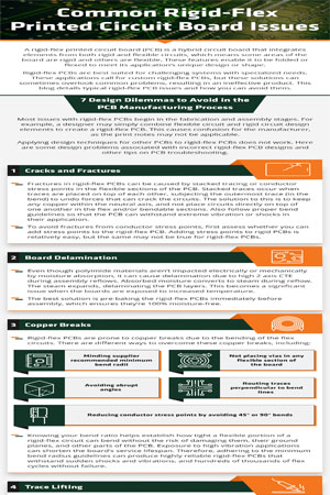
A rigid-flex printed circuit board (PCB) is a hybrid circuit board that integrates elements from both rigid and flexible circuits, which means some areas of the board are rigid and others are flexible. These features enable it to be folded or flexed to meet its application’s unique design or shape.
Rigid-flex PCBs are best suited for challenging systems with specialized needs. These applications call for custom rigid-flex PCBs, but these solutions can sometimes overlook common problems, resulting in an ineffective product. This blog details typical rigid-flex PCB issues and how you can avoid them.
7 Design Dilemmas to Avoid in the PCB Manufacturing Process
Most issues with rigid-flex PCBs begin in the fabrication and assembly stages. For example, a designer may simply combine flexible circuit and rigid circuit design elements to create a rigid-flex PCB. This causes confusion for the manufacturer, as the print notes may not be applicable.
Applying design techniques for other PCBs to rigid-flex PCBs does not work. Here are some design problems associated with incorrect rigid-flex PCB designs and other tips on PCB troubleshooting.
Cracks and Fractures
Fractures in rigid-flex PCBs can be caused by stacked tracing or conductor stress points in the flexible sections of the PCB. Stacked traces occur when traces are placed on top of each other, subjecting the outermost trace (in the bend) to undo forces that can crack the circuits. The solution to this is to keep any copper within the neutral axis, and not place circuits directly on top of one another in the flex and/or bendable sections. Also follow proper bend guidelines so that the PCB can withstand extreme vibration or shocks in their application.
To avoid fractures from conductor stress points, first assess whether you can add stress points to the rigid-flex PCB. Adding stress points to rigid PCBs is relatively easy, but the same may not be true for rigid-flex PCBs.
Board Delamination
Even though polyimide materials aren’t impacted electrically or mechanically by moisture absorption, it can cause delamination due to high temperatures during assembly reflows. Absorbed moisture converts to steam during reflow. The steam expands, delaminating the PCB layers. This becomes a significant issue when the boards are exposed to increased temperature.
The best solution is pre-baking the rigid-flex PCBs immediately before assembly, which ensures they’re 100% moisture-free.
Copper Breaks
Rigid-flex PCBs are prone to copper breaks due to the bending of the flex circuits. There are different ways to overcome these copper breaks, including:
- Minding supplier recommended minimum bend radii
- Not placing vias in any flexible section of the board
- Reducing conductor stress points by avoiding 45° or 90° bends
- Avoiding abrupt angles
- Routing traces perpendicular to bend lines
Knowing your bend ratio helps establish how tight a flexible portion of a rigid-flex circuit can bend without the risk of damaging them, their ground planes, and other parts of the PCB. Exposure to high vibration applications can shorten the board’s service lifespan. Therefore, adhering to the minimum bend radius guidelines can produce highly reliable rigid-flex PCBs that withstand sudden shocks and vibrations, and hundreds of thousands of flex cycles without failure.
Trace Lifting
Trace lifting occurs when copper traces on the surface of the PCB are mechanically stressed. The trace may get lifted from the circuit, causing it to fail. To solve this problem, increase the traces’ surface area, so they can have enough space to adhere to the outerlayers.
Drilling Through Adhesive Layers
Drilling through acrylic adhesives, that are commonly used in flexible coverlayers and bondplies, can increase the risk of via failure. The acrylic resin in these materials have very high Z axis CTE expansion rates, which can put enormous stress on your plated through holes. To reduce this risk, manufacturers of high reliability rigid flex use a technique called cut back coverlayer. The coverlayer and/or bonply that covers the circuits in the flexible sections of the PCB, extends .050” (1.27) mm into the rigid boards, but no more. The coverlayer or bondply is then mated up with a sheet of no flow prepreg in the rigid board. Vias which are near the rigid to flex transition area, are drilled at least .050” (1.27mm) away from the transition line. This ensures that the drilled vias are going through laminate and prepreg and not the acrylic adhesive layers. See IPC 2223 5.2.2.2 and 5.2.2.3 to learn more about the requirements of this design area.
Board Warping From Asymmetrical Construction
Some rigid-flex PCB designers use asymmetrical material layup, which means the flexible layers are not in the center. For instance, making layers four and five flexible in a six-layer rigid flex board can cause the PCB to warp. IPC 2223 Sectional Standard on Flexible Circuit Design advises against asymmetrical designs, recommending designers keep flexible layers centered as much as possible.
Reduced PCB Yields Caused by Dual Finishes
Dual finishes—where there are two different kinds of finishes on the same board—are common with rigid boards. Sometimes rigid-flex PCB designers prefer using electroless nickel immersion gold (ENIG) on most features but hard nickel or gold finishes for the dome switches and edge connectors. However, this should be avoided with rigid-flex PCBs.
Dual finishes can make imaging and protecting underlying features difficult, since rigid-flex PCBs usually have a lot of topography. Plus, dual finishes can reduce rigid-flex PCB yields, so designers should stick to a single finish whenever possible.

